|
Joseph Tarango |
||
|
Home
|
||
Lab 4: AVR Hardware & Calculator with keypad input.PART 1In this lab we will be configuring your physical AVR microcontroller for the first time. Step 1 is to build the circuit below on your breadboard. For more information on pinout of the AVR microcontroller, see the AVR datasheet here. The datasheet will be your best friend for the rest of the quarter, so it would be useful to learn how to navigate it.All resistances are 330 Ohms. 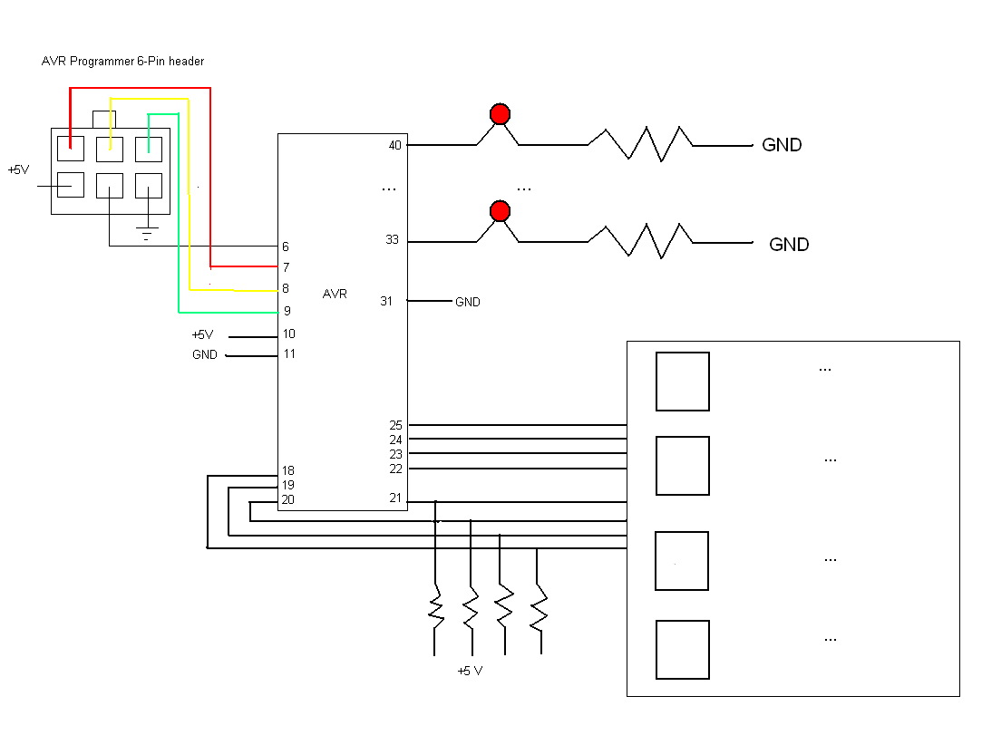 Step 2 is to configure your AVR for use for the first time. Open AVR Studio and start a new project following the protocol given in lab 1. Build the following code: SAMPLE CODE:
Once the code above successfully compiles, select Tools->Program
AVR->Connect to bring up the dialog box below. Ensure the below options
are selected, and that your programmer is plugged into your machine
via USB cable. Part 2Lab 3 we will be implementing a simple calculator with 4 functions. We will use the keypad as input to the design. You must use the state machine format provided in lab 3 to implement your design, and a large percentage of your grade will depend on you using the correct format. Remember that this is a course in embedded system DESIGN, as well as in programming, thus you should have a complete state machine design in pen and paper BEFORE you start to write code.Here is how a user should be able to use the calculator.
KEYPAD INPUTKeypads are often used as a primary input device for embedded microcontrollers. The keypads actually consist of a number of switches, connected in a row/column arrangement as shown below In order for the microcontroller to scan the keypad, it outputs a nibble to force one (only one) of the columns low and then reads the rows to see if any buttons in that column have been pressed. The rows are pulled up by the internal weak pull-ups in the AVR ports. Consequently, as long as no buttons are pressed, the microcontroller sees a logic high on each of the pins attached to the keypad rows. The nibble driven onto the columns always contains only a single 0. The only way the microcontroller can find a 0 on any row pin is for the keypad button to be pressed that connects the column set to 0 to a row. The controller knows which column is at a 0-level and which row reads 0, allowing it to determine which key is pressed. For the keypad, the pins from left to right are: R1, R2, R3, R4, C1, C2, C3, C4.  Below is the start of a function that you should use to get input from the keyboard. You will need to complete the function. The function would be most helpful if it returned an index into the following conversion table. SAMPLE CODE:
PORT/PIN Registers (PORT is for writing! PIN is for reading!) Note that when reading an input from the pins of an AVR, we use the PIN registers of the corresponding port (as opposed to PORT register). Thus to write a value x as an output to port C we would use the statement "PORTC = x", and to read an input value into a variable x on port d we would use the statement "x = PIND".The nuanced difference between the PORT and PIN registers is that PIN register always reflects the current level on the pins of the microcontroller port (subject to both writing from software and voltage levels on the breadboard), whereas the PORT register will return only the last value that you wrote to it. This means that the breadboard hardware could change the logical level of the pins of the port, but the PORT register would not recognize that. POST LABINDIVIDUALLY prepare and submit a single-spaced half page report with the following information.I. Lab Objective II. Personal Contributions III. Skill learned & knowledge gained. TurninINDIVIDUALLY prepare and submit all lab files into a tar ball. All .c files should be included in lab parts, as well as post lab submitted in pdf and txt format. All files should include a header with name, login, email, lab section, assignment, and group associates; also include: "I acknowledge all content is original."For Example Name: John Doe Login: jdoe Email: jdoe@cs.ucr.edu Lab Section: 021 Assignment: Lab 4 Group: John Doe, Jane Doe, and Joe Doe I acknowledge all content is original. Tar ball command: tar -cvzf name.tgz *.c *.pdf *.txt The tar command will compress all files into a .tgz file with all .c .pdf, and .txt files in that directory. Do not include unnecessary files! The .c files be named as follows lab#_part#.c and the postlab#.pdf/postlab#.txt. For Example: lab4_part1.c lab4_part2.c postlab4.pdf postlab4.txt |

